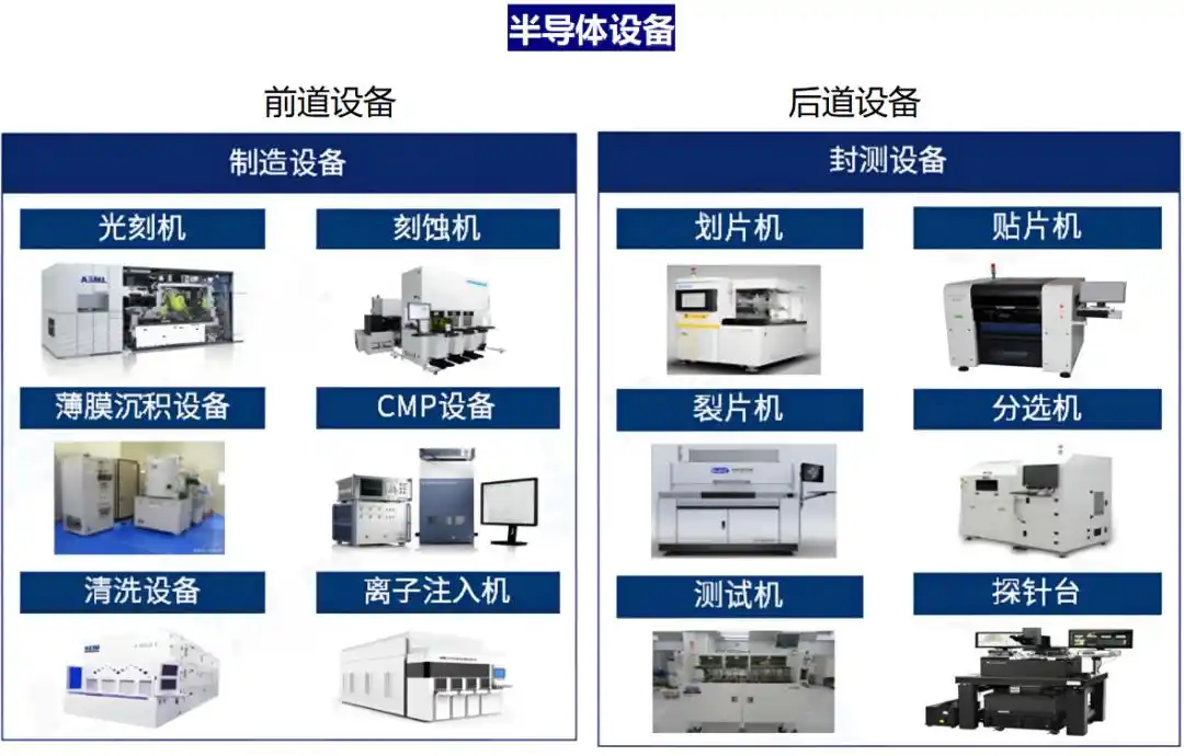
2026年10月14—16日,2026湾区半导体产业生态博览会(简称“湾芯展”)将在深圳会展中心(福田)举办,同期举办国际半导体设备技术与工艺论坛!
当摩尔定律迈向埃米尺度,半导体产业正面临先进制程微缩与成熟制程提质的双重命题。湾芯展将专设国际半导体设备技术与工艺论坛,围绕逻辑芯片、存储芯片等晶圆加工,探讨产业趋势、前沿技术、应用需求与工程化落地,邀请学术界和产业界嘉宾分享最新研究成果与实践经验。

产业生态合作伙伴


赞助合作
WESEMiBAY 2026
议程抢先一览

WESEMiBAY 2026
嘉宾阵容揭晓



演讲简介/亮点
本演讲汇报研究团队在兆声波清洗系统国产化研发与产业化成果,包括:(1)基于有限元的兆声波清洗系统仿真建模与实验测试。(2)自研兆声波系统的核心技术与系列产品。(3)工艺应用案例。团队研发产品可助力我国半导体晶圆制造的超洁净湿法清洗能力。
This presentation summarizes the research team’s achievements in the domestic R&D and industrialization of Megasonic cleaning systems, including:(1) Finite-element-based simulation modeling and experimental testing of Megasonic cleaning systems.(2) Core technologies and product portfolio of self-developed Megasonic systems.(3) Process application cases.The team’s developed products can help enhance the ultra-clean wet cleaning capability for semiconductor wafer manufacturing in China.


演讲简介/亮点
围绕晶圆制造中产能与良率这一核心命题,本次演讲将结合晶合集成AI应用与智能制造实践,分享如何从实际生产问题出发,将AI技术导入良率提升、制程优化与制造管理场景,并探讨晶圆厂如何从经验改善走向数据与AI协同优化,持续释放制造效能。


演讲简介/亮点
演讲立足化合物半导体产业快速发展的时代背景,系统梳理了氮化镓、碳化硅、砷化镓等化合物半导体材料在通信、新能源汽车、光伏储能、算力卫星等关键领域的应用现状与市场前景;深入剖析了化合物外延设备在缺陷控制、新材料兼容等方面的工艺技术挑战。结北方华创在外延领域的核心技术与产业化实践,分享了公司的系统性解决方案与创新成果。
Grounded in the era of rapid growth in the compound semiconductor industry, this presentation systematically reviews the current applications and market prospects of compound semiconductor materials—such as GaN, SiC, and GaAs—in key fields including telecommunications, new energy vehicles, photovoltaic energy storage, and satellite computing. It also provides an in-depth analysis of the process and technological challenges facing compound semiconductor epitaxy equipment, such as defect control and compatibility with new materials. Drawing on NAURA's core technologies and industrialization practices in the epitaxy field, the presentation shares the company's systematic solutions and innovative achievements.


演讲简介/亮点
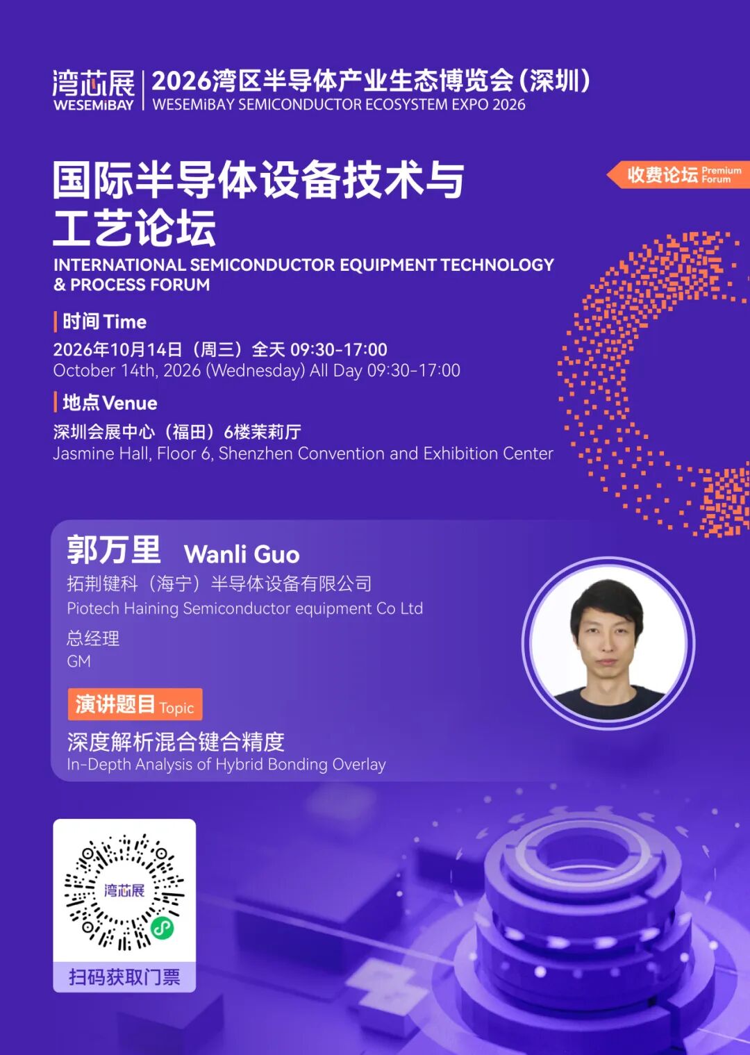
随着三维集成技术向更小互连间距快速演进,对混合键合精度提出更高的要求。报告从Alignment Error、Scaling、Residual三大误差项切入,系统分析其来源、改善方法及W2W与D2W之间的差异。最后总结拓荆键科在混合键合领域的产品布局与技术方向。



演讲简介/亮点
随着智能手机摄像头对更高图像质量的需求不断增长,CMOS图像传感器(CIS)技术正快速演进,朝着更高分辨率、更低信噪比(SNR)以及更强的图像处理能力发展。更高分辨率意味着像素尺寸缩小,这将导致每个像素的入射光减少并增加像素间串扰。为确保小像素具有足够的满阱容量(FWC),需要增加有源硅厚度,这要求采用更高纵横比的深沟槽隔离(DTI)技术来抑制串扰。实现更低的SNR需要降低暗电流和白像素(white pixel)水平,这要求在加工过程中尽量减小等离子体诱导损伤(PID)和金属污染水平。最后,在CIS制造中开发并应用混合键合技术,可将逻辑和DRAM晶圆与像素晶圆集成,从而增强图像处理能力。本文将讨论CIS技术的演进及其关键技术挑战。Lam Research正为先进CIS应用提供多种制造解决方案:针对背面DTI,Lam Syndion®系列支持快速气体切换、低温(Cryo)静电卡盘(ESC)和超低偏压,实现高纵横比的背面DTI刻蚀并将PID降至最低;Lam Striker®系列提供低应力的ALD间隙填充能力,以满足高纵横比DTI需求。在金属污染控制方面,Lam Kiyo®系列配备先进的生产力套件和Corvus® R,通过减少破真空次数,在前端工艺(FEoL)中实现低金属污染水平;Lam Equipment Intelligence®与数据分析(EI DA)利用大数据与机器学习分析半导体制造数据,并通过光发射光谱(OES)数据分析,在CIS制造中实现金属污染监控与改进的过程控制。对于混合键合工艺,Lam Vector®系列提供具有高键合强度且具备优异铜金属化扩散阻挡性能的NDC薄膜;Lam Vector® DT与Coronus®系列能够在不接触正面的情况下进行背面沉积,并允许在倒角区域进行刻蚀/沉积处理,从而改善混合键合工艺中的晶圆应力与倒角缺陷控制,提升CIS制造良率。
With the growing demand for higher image quality from smartphone cameras, CMOS image sensor (CIS) technology is rapidly evolving towards higher resolution, lower signal-to-noise ratio (SNR), and enhanced image processing capabilities. Higher resolution implies CIS pixel size scaling, which leads to reduced incident light per pixel and increased crosstalk between pixels. To ensure sufficient full-well capacity (FWC) for smaller pixels, the active silicon thickness must be increased, necessitating the challenging deep trench isolation (DTI) technology with a higher aspect ratio for crosstalk suppression. Achieving a lower SNR requires the reduction of dark current and white pixel levels, which demands minimized plasma-induced damage (PID) and metal contamination level during processing. Finally, the development and utilization of hybrid bonding technology in CIS manufacturing enables the integration of logic and DRAM wafers with pixel wafers, thereby enhancing image processing capabilities. In this report, we will discuss the evolution of CIS technology and the key technical challenges. Lam Research is offering various manufacturing solutions for advanced CIS applications. For backside DTI, Lam Syndion® series support rapid gas switching, cryo temperature ESC, and ultra-low bias, achieving high aspect ratio backside DTI etching with minimal PID; Lam Striker® series provides low stress ALD gapfill capability to meet high aspect ratio DTI requirement. For metal contamination control, Lam Kiyo® series is equipped with advanced productivity kits and Corvus® R, enabling low metal contamination levels with reduced vacuum breaks in FEoL processes; Lam Equipment Intelligence® and Data Analytics (EI-DA) leverage big data and machine learning to analyze semiconductor manufacturing data and achieve metal contamination monitoring and improved process control through optical emission spectroscopy (OES) data analysis in CIS manufacturing. For hybrid bonding processes, Lam Vector® series provides NDC films with high bonding strength and excellent copper metallization diffusion barrier properties; Lam Vector® DT and Coronus® series enable the backside deposition without contacting the front side and allow etching/deposition processing in the bevel area, thereby improving the wafer stress and bevel defect control in the hybrid bonding processes to enhance the yield of CIS manufacturing.



演讲简介/亮点
介绍EBARA在中国的历史,主要产品特色等,以及在大湾区的布局。
An introduction to EBARA’s history in China, the key features of its products, and its presence in the Greater Bay Area.



演讲简介/亮点
长期以来,先进工艺加工技术都是支持芯片行业的高速发展的基石,尤其近年来芯片行业微型化、精细化、立体化和集成化的发展趋势,更是对于先进工艺加工技术提出了更高的要求和挑战。为了应对这些挑战,离子束技术也不断推陈出新,演进出了多种发展方向。
在本报告中,鲁汶仪器将会回顾离子束技术的历史和原理,介绍多种新型离子束技术及其在先进工艺领域,尤其是存储领域的尖端应用,同时也会汇报鲁汶仪器在离子束技术方向的最新进展。
For a long time, advanced process technologies have served as the cornerstone supporting the rapid development of the semiconductor chip industry. In particular, the recent trends toward miniaturization, higher precision, three-dimensional integration, and greater functional density have imposed ever-increasing demands and challenges on advanced process technologies. To address these challenges, ion beam technology has been continuously innovating and evolving along multiple developmental paths.
In this report, Leuven Instruments will review the history and fundamental principles of ion beam technology, introduce several novel ion beam techniques and their cutting-edge applications in advanced process nodes—especially in the memory sector—and also present the latest progress made by Leuven Instruments in the field of ion beam technology.



演讲简介/亮点
半导体芯片制造缺陷检测技术及设备背景、痛点,难点。
Background, challenges, and difficulties in semiconductor chip manufacturing defect detection technology and equipment.



演讲简介/亮点
本演讲以半导体设备企业的客户交付与持续服务承诺为主线,提出由履约统筹、国际物流、全球关务、目的地运营、售后备件与逆向物流、供应链资源与金融协同构成的全球履约能力框架,并说明如何将上述能力组织成可复制的跨境履约体系。
This presentation presents a global fulfillment framework for semiconductor equipment companies, covering planning, international logistics, trade compliance, destination operations, after-sales logistics, and supply-chain resource and financial coordination. It shows how these capabilities can support repeatable cross-border delivery and long-term service commitments.

WESEMiBAY 2026
10月相聚深圳湾芯展
诚邀学术界、产业界与投资界的专业观众莅临现场,与嘉宾共同交流半导体设备技术与工艺领域的技术进展、应用机遇与产业实践。

扫码加入论坛交流群
*更多嘉宾及议程信息将陆续公布,最终安排以现场公布为准。欢迎扫码加入论坛交流群,及时获取议程更新与现场动态。

点击“阅读原文”,快速进入湾芯展观众报名通道!