湾芯展将于2026年10月14日至16日在深圳会展中心(福田)举行。展会同期,由深圳市半导体与集成电路产业联盟、深圳先进电子材料国际创新研究院、高性能芯片互联技术联盟(HIPI联盟)主办的“国际先进封装工艺与材料论坛暨第三届集成电路材料产业发展论坛”,将于10月15日在深圳会展中心(福田)6楼水仙厅举行。
AI算力、高速互连与Chiplet异构集成推动先进封装向工艺、材料与量产协同发展。本次论坛聚焦2.5D/3D集成、Chiplet封装、混合键合、TSV/TGV、RDL重布线、Fan-Out、SiP、存储器先进封装及CPO/高速光互连等关键工艺路径,以及光刻胶、特气、靶材、塑封料、量测、热管理和高纯流体管路等关键环节,交流材料验证、工艺适配与国产供应链导入。

产业生态合作伙伴

赞助合作

WESEMiBAY 2026
议程抢先一览

WESEMiBAY 2026
嘉宾阵容揭晓


演讲简介/亮点
廖武刚,深圳大学集成电路学院长聘副教授、博士生导师,深圳市半导体异质集成技术重点实验室副主任。研究聚焦半导体器件与异质异构集成技术,主编《异质异构集成封装技术》。



演讲简介/亮点
随着摩尔定律逐步逼近物理极限,先进封装技术已成为延续并拓展芯片性能的关键路径。在先进封装制程中,光刻胶材料承担图形化转移与介质层构建的核心功能,其性能直接影响封装的精度、可靠性与良率。其中,光敏聚酰亚胺(PSPI)与厚膜光刻胶是两类最具代表性的关键材料——前者广泛用作重分布线层(RDL)的绝缘介质、应力缓冲层及钝化保护层,后者主要用于凸块(Bump)制造的电镀掩膜。长期以来,这两款核心材料被美日企业高度垄断,国产化替代需求十分迫切。
深圳职业技术大学集成电路关键材料研究院团队从光刻胶底层树脂的分子结构设计入手,依托可靠的纯化与可控聚合技术,系统开展配方体系的设计与优化,并结合大量工艺匹配性验证,成功开发出本征特性和光刻性能优异、工艺适配性和可靠性高的光敏聚酰亚胺和厚膜光刻胶材料,实现了相关材料的国产化突破。
As Moore's Law approaches its physical limits, advanced packaging technology has become the key path to continue and expand the performance of chips. In advance-d packaging processes, photoresist materials undertake the core functions of pattern transfer and dielectric layer construction, and their performance directly determines packaging accuracy, reliability, and yield of the packaging. Among them, photosensitive polyimide (PSPI) and thick-film photoresist are two of the most representative key materials—the former is widely used as insulating dielectrics for redistribution layers (RDL), stress buffer layers, and passivation layers, while the latter is primarily employed as electroplating masks for bump manufacturing. For a long time, these two critical materials have been highly monopolized by enterprises from the United States and Japan, and there is an urgent need for domestic substitution.
The research team from the Institute of Critical Materials for Integrated Circuits at Shenzhen Polytechnic University started with molecular structure design of the underlying resin of the photoresist. Through reliable purification and controllable polymerization technologies, we systematically optimized the formulation and carried out extensive process compatibility testing. Finally, we successfully developed photo-sensitive polyimide and thick film photoresist materials with excellent inherent characteristics and outstanding lithographic performance, as well as high process adaptability and reliability. Through these efforts, we have achieved a pivotal breakthrough in the localization of these essential photoresist materials.



演讲简介/亮点
超高纯靶材在先进逻辑和先进存储的最新应用;2.5D/3D先进封装超高纯靶材的应用趋势。
Latest Applications of Ultra-High-Purity Targets in Advanced Logic and Advanced Memory; Application Trends of Ultra-High-Purity Targets for 2.5D/3D Advanced Packaging.



演讲简介/亮点
大尺寸金刚石是其从“未来材料”走向“核心材料”的必经之路。金刚石被誉为“终极半导体材料”,其热导率高达2000—2200 W/(m·K),约为铜的5倍;在高温、高频、高功率及抗辐射等极端环境的应用不可替代。郡瑞科技具备30mm大尺寸单晶,12寸多晶的规模化量产能力。
Large-sized diamonds are an essential step in transitioning from "future materials" to "core materials." Diamond is hailed as the "ultimate semiconductor material," with a thermal conductivity as high as 2000–2200 W/(m·K), approximately five times that of copper, making it irreplaceable in extreme environments such as high temperature, high frequency, high power, and radiation resistance. Junrui Technology Co.,Ltd. has already achieved large-scale production capabilities for 30 mm large single crystals and 12-inch polycrystals.



演讲简介/亮点
高性能PTFE与高纯PFA管路的工艺提升与自主可控。
Process Optimization and Supply Chain Independence of High-Performance PTFE and Ultra-High-Purity PFA Tubing.



演讲简介/亮点
本演讲从半导体检测需求变化出发,解读行业最新进展。内容涵盖检测行业的伴生、杠杆、贯穿与双重效应;先进工艺、半导体装备及零部件、硅光芯片、先进封装与 CPO 四大重点赛道的发展趋势;以及离子注入、薄膜沉积、光刻刻蚀等设备的检测解决方案,结合 SEMI 认证、金属材料检测与零部件失效分析等实战案例。


演讲简介/亮点
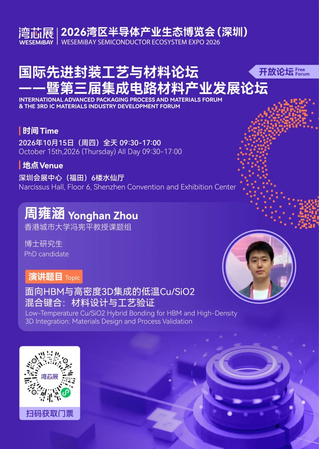
随着HBM、Chiplet及3D集成持续提高互连密度,传统微凸点技术逐渐受到互连间距与热预算的双重限制。 Cu/SiO2混合键合能够提供高密度、低寄生的垂直互连,但其产业化仍依赖低温Cu连接、表面平坦度、工艺窗口及电性可靠性的协同控制。
本报告将介绍一种结合纳米晶活性与孪晶结构稳定性的低温Cu材料,并围绕“材料设计—8英寸镶嵌工艺—D2D混合键合—电性与可靠性”开展系统验证。在200 ℃热预算下实现高强度 Cu/SiO2混合连接;8英寸工艺获得4.3%的电镀片内均匀性指标和85.1%的CMP窗口通过率,并完成5 μm Cu/SiO2结构键合。六组抽测样品的初始有效导通率达到83.3%–95.8%,代表性Kelvin及Daisy-chain结构在135 ℃、1–2×10⁶ A/cm²高温高电流条件下持续导通超过30天。
低温Cu材料有着优异的工业级性能,为HBM、Chiplet和高密度3D集成应用提供优良选择,为进一步建立晶圆级良率、扩大样本规模和推进产业化奠定坚实基础。
As HBM, chiplets, and 3D integration continue to drive higher interconnect densities, conventional microbump technologies are increasingly constrained by interconnect pitch and thermal budget. Cu/SiO2 hybrid bonding enables high-density vertical interconnects with low parasitics. However, its industrial implementation still requires coordinated control of low-temperature Cu bonding, surface planarity, process windows, and electrical reliability.
This presentation introduces a low-temperature Cu material that combines the high bonding activity of nanocrystalline Cu with the structural stability of nanotwinned Cu. Systematic validation was conducted across materials design, 8-inch damascene processing, die-to-die hybrid bonding, electrical characterization, and reliability testing. High-strength Cu/SiO2 hybrid-bonded interfaces were achieved at a thermal budget of 200 °C. The 8-inch process demonstrated a within-wafer electroplating uniformity metric of 4.3%, an 85.1% CMP process-window pass rate, and successful bonding of 5 μm Cu/SiO2 structures. Six groups of sampled devices exhibited initial conductive yields ranging from 83.3% to 95.8%. Representative Kelvin and daisy-chain structures remained electrically conductive for more than 30 days at 135 °C under high current densities of 1–2 × 10⁶ A/cm².
The low-temperature Cu material demonstrates strong potential for industrial applications and provides a promising interconnect option for HBM, chiplets, and high-density 3D integration. These results also establish a solid foundation for further wafer-level yield evaluation, expansion of the sample size, and future manufacturing scale-up.
WESEMiBAY 2026
10月相聚深圳湾芯展
诚邀学术界、产业界与投资界的专业观众莅临现场,与嘉宾交流先进封装工艺、材料技术及产业导入实践。

扫码加入论坛交流群
*更多嘉宾及议程信息将陆续公布,最终安排以现场公布为准。欢迎扫码加入论坛交流群,及时获取议程更新与现场动态。

点击“阅读原文”,快速进入湾芯展观众报名通道!