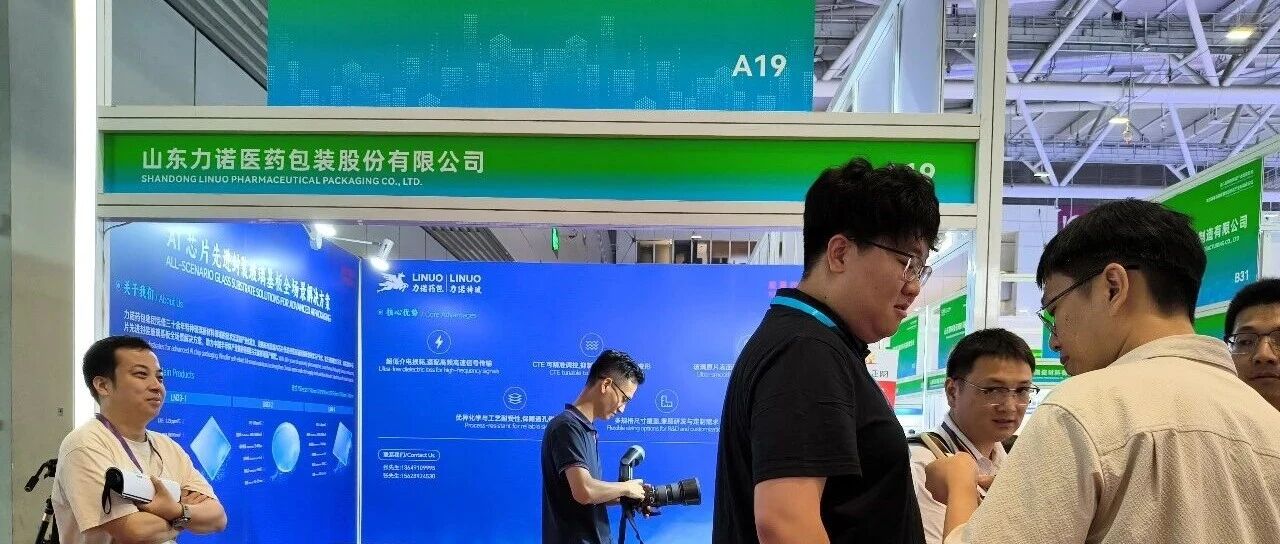
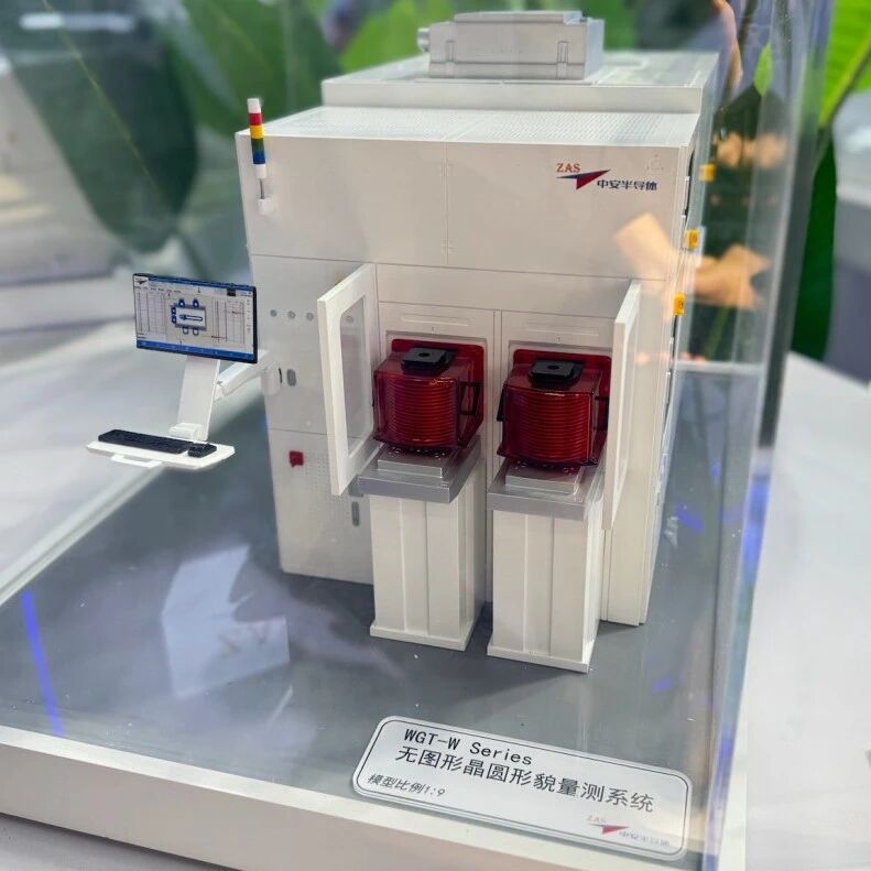
湾芯展将于2026年10月14日至16日在深圳会展中心(福田)举行。展会同期,在第三代半导体国家技术创新中心指导下,由深圳市半导体与集成电路产业联盟、深圳平湖实验室共同主办的化合物及功率半导体系列论坛将精彩启幕。
粤港澳大湾区汇聚新能源汽车、数据中心及科技应用产业,对化合物半导体和功率半导体技术形成旺盛需求。湾芯展将专设化合物及功率半导体展区与系列论坛,围绕化合物半导体及硅基功率半导体,集中探讨产业趋势、前沿技术、应用需求与工程化落地,邀请学术界和产业界嘉宾分享最新研究成果与实践经验。

产业生态合作伙伴

WESEMiBAY 2026
议程抢先一览

WESEMiBAY 2026
嘉宾阵容揭晓


演讲简介/亮点
超宽禁带半导体相较于当前产业化主流半导体材料,拥有跨代际物理特性优势,具有不可替代的战略价值。本演讲主要围绕超宽禁带半导体技术与发展现状,在介绍其优异性能和广阔应用前景的同时,结合政策布局、产业现状分析思考当前面临的技术、市场、产业困局,形成几点认识供交流研讨。
Ultra-wide bandgap semiconductors (UWBGS), endowed with cross-generational physical property advantages compared with the currently mainstream commercial semiconductor materials, hold significant and irreplaceable strategic value for international technological competition. Based on the technology and development status of the UWBGS, this presentation introduces their outstanding performance and broad application prospects, also analyzes the current technical, market and industrial dilemmas in the context of current policy and industry landscapes. Finally, we offer some viewpoints for discussion.



演讲简介/亮点
氮化镓功率器件正成为 AI 数据中心(AIDC)下一代电力传输与供电系统的关键使能技术。随着计算密度的快速提升,AIDC 对更高效率、更高功率密度、更快瞬态响应以及更优热管理提出了迫切需求。GaN 功率晶体管已从实验室原型发展到广泛的商业化应用,其高频开关能力突破了硅器件的实际极限,使紧凑、高效的功率变换器成为可能。为了进一步发挥 GaN 在 AIDC 电源架构中的本征优势,器件与电路创新必须从分立的横向晶体管,逐步演进到多维度 GaN 功率技术,包括横向、垂直、双向、异质集成以及单片集成器件平台。
本报告将围绕“面向功能的集成”这一核心,讨论用于高功率密度电能变换的 GaN 功率集成基础及其最新进展。GaN CMOS、双向 GaN 开关,以及将 GaN 沟道输运优势与 SiC 垂直耐压能力相结合的混合 GaN/SiC HyFET 等新兴概念,预示着未来功率晶体管将不再只是单一开关器件,而是演变为具备多功能、保护能力、热感知能力,并有望具备数据感知与传输能力的系统节点。这些多维度器件与集成方法,为面向 AIDC 基础设施快速增长能源需求的可扩展、高可靠、智能化电力电子技术提供了有前景的发展路径。
Gallium nitride power devices are becoming key enablers for next-generation power delivery in AI data centers (AIDCs) where rapidly increasing computing density demands higher efficiency, higher power density, faster transient response, and improved thermal management. GaN power transistors have advanced from laboratory prototypes to broad commercial adoption, enabling compact and efficient power converters through high-frequency switching beyond the practical limits of silicon. To further exploit GaN’s intrinsic advantages for AIDC power architectures, device and circuit innovation must evolve from discrete lateral transistors toward multi-dimensional GaN power technologies, including lateral, vertical, bidirectional, heterogeneous, and monolithically integrated device platforms.
This talk discusses the foundations and recent progress of GaN power integration for high-density power conversion by emphasizing on integration for functionality. Emerging concepts such as GaN-based CMOS, bidirectional GaN switches, and hybrid GaN/SiC HyFETs that combine GaN channel transport with SiC vertical blocking capability point toward a future in which the power transistor becomes a multifunctional, protected, thermally aware, and potentially data-enabled system node. These multi-dimensional device and integration approaches offer promising pathways for scalable, reliable, and intelligent power electronics tailored to the rapidly growing energy demands of AIDC infrastructure.



演讲简介/亮点
新能源车车载功率系统,持续向着小型化、高集成、高可靠方向迭代。方正微电子推出 DIP32 新一代功率模组,面向车载功率场景,可应用于压缩机控制、主动悬架、OBC/DCDC 等车载单元;集成化封装简化整机设计,满足严苛车规可靠性标准,助力客户加速产品落地。
New energy vehicle on-board power systems are continuously evolving toward miniaturization, higher integration and higher reliability. Founder Microelectronics launches the new-generation DIP32 power module for automotive power applications. It is widely adopted in compressor control, active suspension, OBC and DC-DC systems. With highly integrated packaging, the module simplifies overall system design, complies with stringent automotive reliability standards, and accelerates product deployment for customers.



演讲简介/亮点
化合物半导体(GaAs、InP、SiC、GaN、Ga₂O₃等)是支撑AI算力、光通信、空间光伏、新能源与射频微波等前沿领域的核心材料体系,其器件性能持续牵引外延、氧化、退火等关键制造工艺不断升级。本报告以器件发展趋势为牵引,简要分析不同材料体系化合物半导体在外延生长及氧化、退火等工艺环节的技术特点与共性瓶颈,明确器件制造对核心装备的功能及性能指标要求。从装备研制视角出发,通过机理分析、模拟仿真与关键零部件正向设计相结合,提出覆盖化合物半导体外延与SiC氧化退火等关键工艺环节的装备解决方案,重点介绍相关装备国产化进程、技术突破与产业化应用进展。
Compound semiconductors—GaAs, InP, SiC, GaN, and Ga₂O₃—constitute a core material platform supporting AI computing, optical communications, space photovoltaics, renewable energy, and RF/microwave applications. The continuous advancement of device performance drives the evolution of critical manufacturing processes, including epitaxial growth, oxidation, and annealing. Guided by device technology trends, this presentation briefly analyzes the process characteristics and shared bottlenecks in epitaxial growth, oxidation, and annealing across different compound semiconductor material systems, and defines the functional and performance specifications required for core manufacturing equipment. From an equipment-development perspective, integrated mechanistic analysis, numerical simulation, and first-principles design of critical components are employed to deliver comprehensive solutions for compound semiconductor epitaxy and SiC oxidation/annealing. Emphasis is placed on localization progress, technological breakthroughs, and industrial deployment.


演讲简介/亮点
GPU性能和功耗越来越高,Scaleup域越来越大,未来趋势是从100KW走向1MW。以终局判断,1MW的超节点,对于供电、液冷、互联都有巨大的挑战。
As GPU performance and power consumption continue to rise and scale-up domains expand, the industry is trending from 100 kW toward 1 MW. From an end-state perspective, a 1 MW supernode poses major challenges for power delivery, liquid cooling, and interconnects.


演讲简介/亮点
算力产业蓬勃发展,推动功率与化合物半导体迈入变革浪潮。随着 AI 算力持续扩张,功率半导体已然成为算力基础设施的核心底座。士兰坚守创新智造之路,深耕功率与化合物半导体赛道,构建“从电网到核心”全链路电源产品解决方案。踏浪前行,与行业伙伴共启芯征程。
The rapid growth of the computing industry is driving change in power and compound semiconductors. As AI computing capacity expands, power semiconductors are becoming a core part of computing infrastructure. Silan continues to invest in manufacturing innovation and in power and compound semiconductor technologies, building end-to-end power solutions “from the grid to the computing core.” Together with industry partners, it aims to advance the next phase of semiconductor development.



演讲简介/亮点
报告梳理国内外10kV以上SiC MOSFET/IGBT研发现状,结合新型电力系统场景,剖析超高压SiC器件的应用进展与落地瓶颈,以深圳平湖实验室超高压SiC器件成果为例,呈现国产超高压SiC器件、材料及工艺阶段性进展。
This talk reviews global progress in 10kV+ SiC MOSFET/IGBT research and development, analyzes application advances and deployment bottlenecks of ultra-high-voltage SiC devices in emerging power system scenarios, and addresses key technology hurdles. Using Shenzhen Pinghu Laboratory's ultra-high-voltage SiC device achievements as a case study, it highlights the staged progress of domestic ultra-high-voltage SiC devices.



演讲简介/亮点
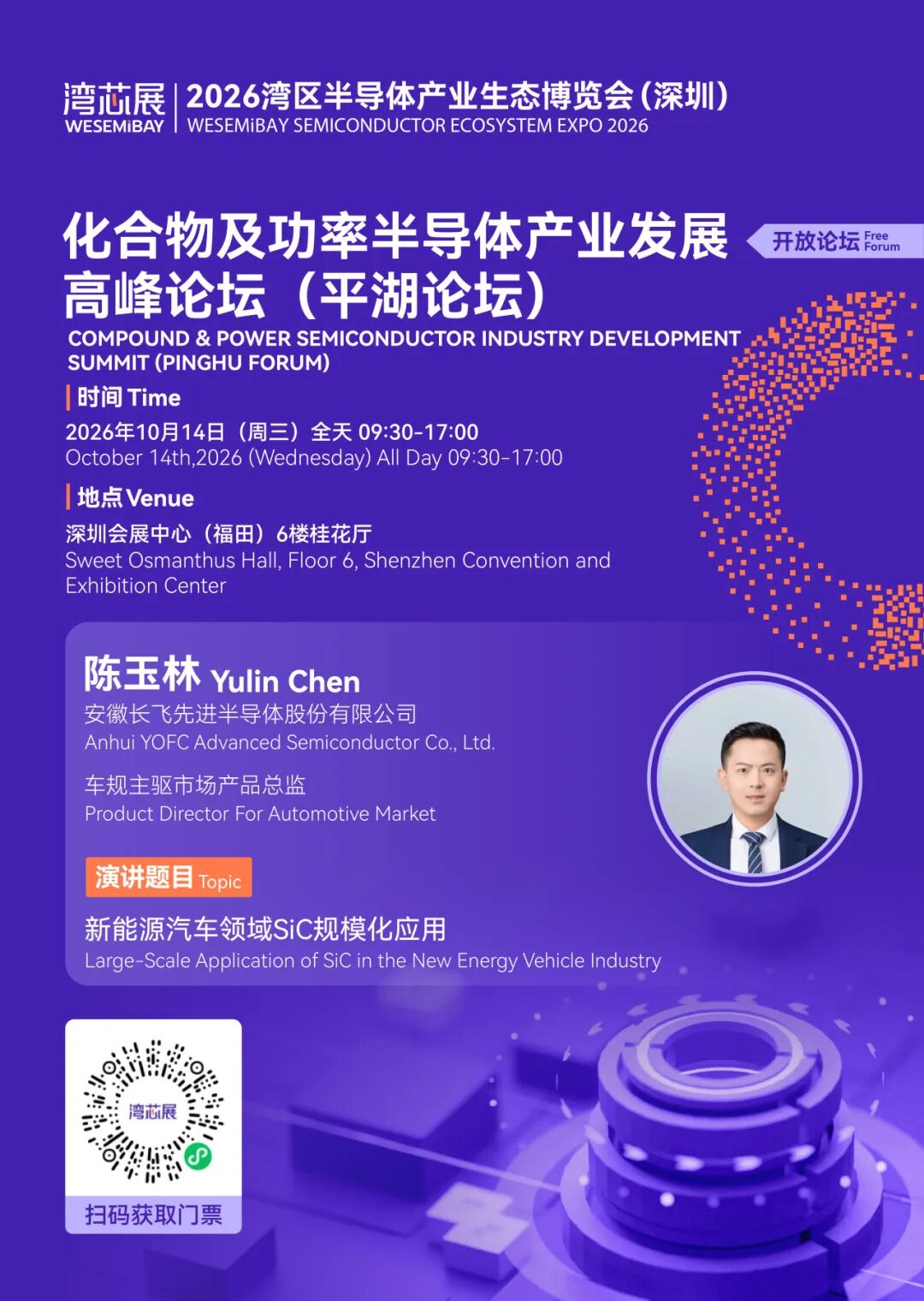
通过介绍汽车级功率半导体SIC MOS在新能源汽车领域的应用现状,提出应用中的问题及批量应用的考量及解决方案,最后对未来发展前景进行了展望。
This speech presents the current application status of automotive-grade SiC MOSFETs in new energy vehicles, analyzes the existing challenges and key considerations for large-scale application, proposes corresponding solutions, and concludes with a prospect of future development trends.


演讲简介/亮点
1. 新能源汽车功率电子产品SiC代Si进展及趋势
2. 远超行业标准的可靠性要求
3. 汽车大规模应用背景下的成本控制
1. SiC Replacing Si in NEV Power Electronics: Progress & Trends
2. Reliability Requirements Far Beyond Industry Standards
3. Cost Control Under Large-Scale Automotive Deployment


演讲简介/亮点
本报告围绕碳化硅(SiC)第三代半导体展开,指出在双碳目标、新能源汽车爆发、AI 算力激增的背景下,传统硅基器件难以满足高压、高频、高效电能转换需求,SiC 凭借高耐压、耐高温、高频高效、高功率密度四大优势,成为新一代电力核心器件。
在新能源汽车领域,SiC 支撑 800V 高压平台,提升电驱效率、增加续航并实现超快充,正从高端车型向主流车型普及,国产 SiC 芯片与车规模块已实现规模化突破。昕感科技拥有芯片设计到封装测试全栈能力,推出多款符合车规标准的 SiC 功率模块。
在 AI 算力领域,SiC 可大幅降低数据中心供电损耗、优化 PUE 值,支撑高压直流供电与固态变压器,成为继电动车后的第二增长曲线。目前中国 SiC 产业链已全面突破,未来将向大尺寸晶圆、沟槽型器件、集成化封装升级,同时亟需材料、电力电子、热学等跨学科复合型人才。
This report examines silicon carbide (SiC) as a third-generation (wide-bandgap) semiconductor. It highlights that amid the global push for carbon peaking and carbon neutrality (the “dual carbon” goals), the rapid expansion of new energy vehicles (NEVs), and the surging demand for AI computing power, conventional silicon-based devices are increasingly unable to meet the requirements for high-voltage, high-frequency, and high-efficiency power conversion. Thanks to four intrinsic strengths—high breakdown voltage, superior thermal tolerance, high-frequency, high-efficiency operation, and high power density—SiC has emerged as the next-generation core power device.
In the NEV sector, SiC enables 800 V high-voltage platforms, improving drivetrain efficiency, extending driving range, and supporting ultra-fast charging. The technology is now transitioning from premium models to mass-market vehicles, while domestic SiC chips and automotive-grade modules have achieved large-scale breakthroughs. NEXIC Technology offers end-to-end capabilities spanning chip design, packaging, and testing, and has launched a portfolio of automotive-grade SiC power modules.
In AI computing, SiC significantly cuts power delivery losses in data centers, optimizes PUE (Power Usage Effectiveness), and supports high-voltage DC power distribution and solid-state transformers—positioning it as the second major growth driver after electric vehicles. At present, China’s SiC industry chain has achieved comprehensive breakthroughs. Looking ahead, the industry will advance toward larger-diameter wafers, trench-gate devices, and advanced integrated packaging, while the urgent need for interdisciplinary talent—combining expertise in materials, power electronics, and thermal management—will only intensify.



演讲简介/亮点
聚焦12吋功率器件技术突破,攻克高质量、高性能的技术难点,赋能车规、AI产业发展,提供覆盖品质管控、性能提升、规模化量产的全套解决方案。
WESEMiBAY 2026
10月相聚深圳湾芯展
诚邀学术界、产业界与投资界的专业观众莅临现场,与嘉宾共同交流化合物及功率半导体领域的技术进展、应用机遇与产业实践。

扫码加入论坛交流群
*更多嘉宾及议程信息将陆续公布,最终安排以现场公布为准。欢迎扫码加入论坛交流群,及时获取议程更新与现场动态。


点击“阅读原文”,快速进入湾芯展观众报名通道!