GAREN

2025年7月,杭州镓仁半导体有限公司(以下简称“镓仁半导体”) 8英寸氧化镓衬底通过了国内/国外知名机构的检测,并联合发布检测结果。
第三方检测结果表明,8英寸衬底XRD摇摆曲线半高宽<30 arcsec,达到国际领先水平。8英寸高质量氧化镓衬底的问世,标志着氧化镓产业化应用迈入全面加速落地阶段,是产业发展的重要里程碑。

深圳平湖实验室
检测结果
本次测试样品为氧化镓8英寸衬底,取点共计5个,XRD摇摆曲线半高宽测试结果:22~26 arcsec。

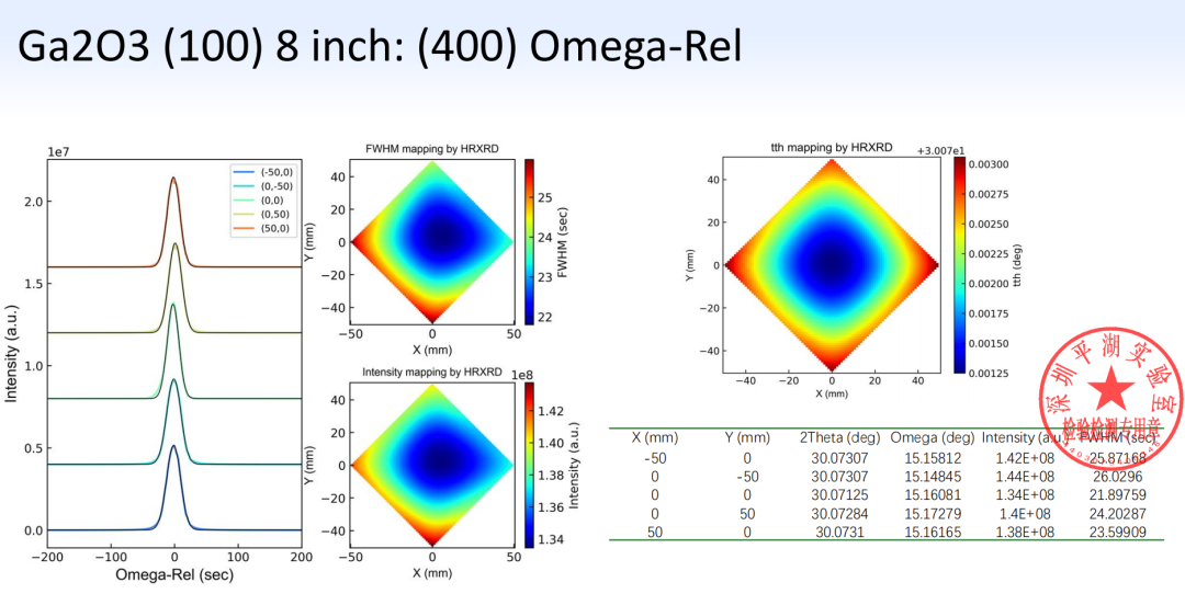
8英寸衬底XRD摇摆曲线半高宽第三方测试结果-(深圳平湖实验室)

马尔文帕纳科亚太卓越应用中心
检测结果
本次测试样品为氧化镓8英寸衬底,取点共计5个,XRD摇摆曲线半高宽测试结果分别为:16.7 arcsec、16.2 arcsec、15.4 arcsec、15.3 arcsec、12.4 arcsec。


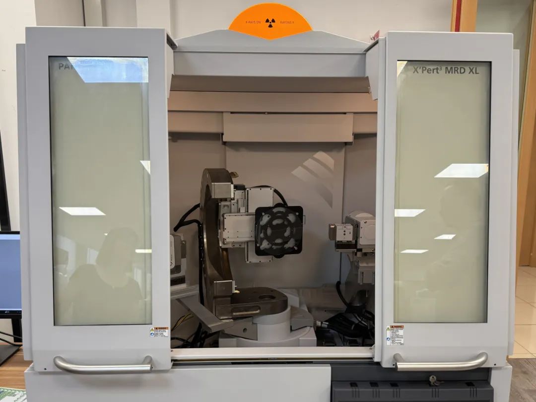
8英寸衬底XRD摇摆曲线半高宽第三方测试结果-(马尔文帕纳科亚太卓越应用中心)


2025年3月,镓仁半导体发布全球首颗第四代半导体氧化镓8英寸单晶,并加工出8英寸衬底,刷新了氧化镓单晶尺寸的全球纪录。中国氧化镓率先进入8英寸时代,具有深远的产业意义:
首先,8英寸氧化镓能够与现有硅基芯片厂的8英寸产线兼容,这将会显著加快其产业化应用的步伐。
其次,氧化镓衬底尺寸增大可提升其利用率,单片晶圆可制造芯片数量呈几何级增长,降低生产成本、提升生产效率。
最后,中国率先突破8英寸技术壁垒,不仅标志着我国在超宽禁带半导体领域的技术进步,更为我国氧化镓产业在全球半导体竞争中抢占了先机,有力推动我国在全球半导体竞争格局中占据优势地位。


目前在售的氧化镓衬底晶圆主要以2英寸和4英寸为主,难以与主流的Fab场产线设备兼容,这提高了下游器件厂商研发的难度与成本,导致氧化镓应用推进缓慢。
本次质量检测结果充分证明,镓仁半导体8英寸晶圆衬底质量优异,能够满足硅基8英寸产线生产要求,这将大幅降低下游应用端研发的难度与成本,促进产业化应用的快速落地。
镓仁半导体氧化镓衬底已逐步实现产业化,为下游客户提供大尺寸高质量的氧化镓单晶衬底产品。目前,镓仁半导体8英寸衬底已实现产品销售出货。


GAREN

In August 2025, Hangzhou GAREN Semiconductor Co., LTD. (hereinafter referred to as "GARENSEMI") announced that its 8-inch β-Ga2O3 substrate had passed inspections conducted by renowned domestic and international institutions, with the test results jointly released.
The third-party testing results indicate that the 8-inch substrate exhibits an XRD rocking curve FWHM of <30 arcsec, achieving the international leading level. The successful development of 8-inch high-quality β-Ga2O3 substrates marks that the industrial application of gallium oxide has entered a stage of accelerated implementation, which is an important milestone in the development of the industry.

TEST RESULTS
-Shenzhen Pinghu Laboratroy
The sample tested was an 8-inch β-Ga2O3 substrate, with a total of 5 measurement points taken. The test results showed the XRD rocking curve FWHM ranged from 22 to 26 arcsec.


Third-party test results of 8-inch substrate XRD rocking curve FWHM
(Shenzhen Pinghu Laboratroy)

TEST RESULTS
- Malvern Panalytical
The sample tested was an 8-inch β-Ga2O3 substrate, with a total of 5 measurement points taken. The XRD rocking curve FWHM were:16.7 arcsec、16.2 arcsec、15.4 arcsec、15.3 arcsec、12.4 arcsec, respectively.


Third-party test results of 8-inch substrate XRD rocking curve FWHM
(Malvern Panalytical)


In March, 2025, GARENSEMI unveiled the world’s first fourth-generation semiconductor 8-inch β-Ga2O3 single crystal and processed it into 8-inch substrates, setting a new global record for the size of β-Ga2O3 single crystals. China’s β-Ga2O3 industry taking the lead in entering the 8-inch era has profound industrial significance:
First, the 8-inch β-Ga2O3 substrate is fully compatible with the existing 8-inch silicon production lines, significantly accelerating the progress of its industrialization.
Second, β-Ga2O3 substrate with larger diameter can remarkably improve its utilization with lower production costs and higher efficiency.


Currently, the commercially available β-Ga2O3 substrate wafers are primarily 2-inch and 4-inch, which are difficult to compatible with mainstream Fab production line equipment. This incompatibility increases the R&D difficulty and cost for downstream device manufacturers, hindering the adoption of β-Ga2O3.
These quality test results fully demonstrate that GARENSEMI's 8-inch wafers substrates exhibit excellent quality and can meet the production requirements of silicon-based 8-inch production lines. This breakthrough will significantly reduce the R&D difficulty and cost for downstream applications, thereby accelerating the industrialization process.
GARENSEMI has gradually achieved the industrialization of gallium oxide substrates, providing downstream customers with large-size, high-quality gallium oxide single crystal substrate products. GARENSEMI has now commenced commercial sales and shipments of its 8-inch substrates.


如需了解更多关于镓仁半导体及其产品的信息
请访问我们的官方网站 :http://garen.cc/
或通过以下方式与我们联系:
江先生:15918719807
邮箱:jiangjiwei@garen.cc
夏先生:19011278792
邮箱:xianing@garen.cc