湾芯展将于2026年10月14日至16日在深圳会展中心(福田)举行。展会同期,由深芯盟主办的“国际半导体材料与晶圆工艺论坛”将于10月14日上午在会展中心5楼牡丹厅举行。
晶圆制造对材料匹配、杂质控制、供应稳定性与量产良率提出持续挑战。本次论坛聚焦大尺寸硅片与石英坩埚、高纯溅射靶材、先进衬底、微污染控制及制造材料解决方案,邀请产业链上下游嘉宾交流技术进展与协同验证实践。

产业生态合作伙伴


赞助合作

WESEMiBAY 2026
议程抢先一览

WESEMiBAY 2026
嘉宾阵容揭晓


演讲简介/亮点
围绕晶圆制造原材料供应链的特点与管理难点、晶圆制造企业与上游供应商的协同重点,以及当前行业发展趋势下的保供风险与解决方案展开交流。
The presentation discusses characteristics and management challenges of wafer manufacturing supply chains, priorities for collaboration between fabs and upstream suppliers, and supply assurance risks and solutions under current industry trends.
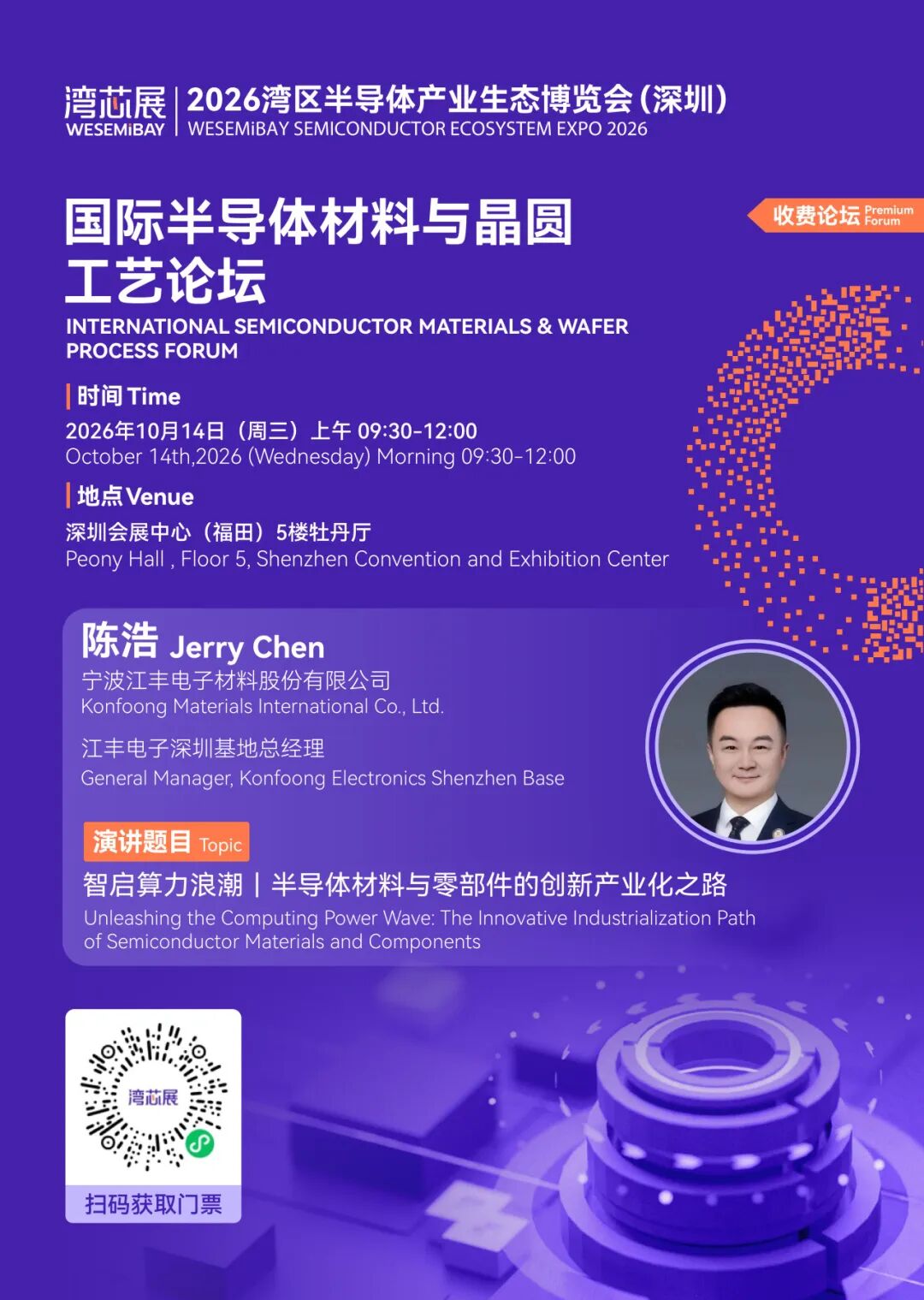


演讲简介/亮点
随着大模型、算力芯片与AI服务器产业高速爆发,全球半导体工艺迭代、设备升级与制造需求进入全新周期,带动半导体高端材料、精密零部件迎来规模化替代机遇。AI高算力芯片对半导体材料和零部件提出更高精度、稳定性、一致性的量产要求,成为推动半导体材料与零部件产业创新突破的核心驱动力。
Fueled by the explosive growth of Large-scale AI model, AI accelerator and the AI server industry, global semiconductor process iteration, equipment upgrading and manufacturing demands have entered a brand new cycle, bringing large scale substitution opportunities for high end semiconductor materials and precision components. High performance AI accelerators impose mass production requirements of higher precision, stability and consistency on semiconductor materials and components, acting as a core driving force for industrial innovation breakthroughs in this industry.


演讲简介/亮点
报告探讨先进光子衬底如何应对人工智能基础设施不断增长的数据传输与能耗需求,介绍从铜互连向光互连转变的产业背景,以及传统硅微缩的局限。重点分享Photon-SOI、Photonics-LNOI和InPOSi等异质集成平台,及其在高带宽密度、能源效率和规模化制造方面的应用潜力。
This presentation explores how advanced photonics substrates serve as the foundational architecture to meet the massive, escalating data and energy demands of modern artificial intelligence infrastructure. It addresses critical datacom market drivers, the industry-wide transition from copper to optical interconnects, and the limitations of traditional silicon scaling. Furthermore, it highlights Soitec's Photon-SOI technology and advanced heterogeneous integration platforms—such as Photonics-LNOI and InPOSi—which seamlessly combine premium materials like thin-film lithium niobate and indium phosphide onto CMOS-compatible silicon handles. Ultimately, the presentation demonstrates how these engineered substrate innovations enable high-bandwidth density, superior energy efficiency, and scalable manufacturing to support the next era of optical networking, hyperscale data centers, and advanced computing applications.


演讲简介/亮点
材料创新正持续推动半导体工艺演进,同时也带来更复杂的微污染控制挑战。面对日益严苛的品质与良率要求,如何有效管理微污染已成为业内关注的重要课题。
本次演讲聚焦微污染控制领域的实践经验与行业洞察,探讨材料创新背景下微污染控制的重要性,以及如何通过整合式微污染控制,协助客户降低缺陷风险并提升产品良率。



演讲简介/亮点
随着逻辑芯片制程持续向先进节点迭代,金属互连、栅极、阻挡层等关键薄膜对电阻率、膜厚均匀性及颗粒缺陷的控制要求日趋严苛。溅射靶材作为PVD工艺核心材料,其晶粒尺寸、晶体织构、内部夹杂及全域组织均匀性,直接影响溅射稳定性、薄膜成核质量与芯片良率。本研究聚焦先进逻辑芯片用高纯铜合金、钽、钴等系列溅射靶材,开展靶材组织与薄膜性能协同调控技术研究,实现靶材微观组织与服役性能的精准、稳定可控,满足14nm 及以下先进制程应用要求。
As logic-chip technology nodes keep advancing, critical thin-films for metal interconnects, gates and barrier layers demand increasingly stringent control over resistivity, thickness uniformity and particle-induced defects. As core materials for PVD processes, sputtering targets with specific grain size, crystallographic texture, internal inclusions and global microstructural uniformity directly govern sputtering stability, thin-film nucleation quality and chip yield. Focusing on high-purity copper-alloy, tantalum and cobalt sputtering targets for advanced-node logic chips, this study investigates synergistic regulation of target microstructure and thin-film performance. It achieves precise, stable control over the microstructure and service performance of targets to meet the requirements of 14 nm-and-below advanced processes.


演讲简介/亮点
分享 3M 面向半导体制造全流程的产品与技术解决方案,覆盖硅片制造、前道制程、中道制程及后道封装等关键环节。重点围绕 CMP、晶圆背面减薄、临时键合等核心工艺,介绍 3M 配套耗材、材料解决方案及应用支持能力,助力提升半导体制造过程中的工艺稳定性、效率与可靠性。
This presentation will introduce 3M’s products and technical solutions across the semiconductor manufacturing value chain, covering wafer manufacturing, front-end, middle-end, and back-end processes. With a focus on key applications such as CMP, wafer backside grinding, and temporary bonding, the session will highlight 3M’s supporting consumables, material solutions, and application expertise that help enhance process stability, efficiency, and reliability in semiconductor manufacturing.


演讲简介/亮点
近年来,国产300mm大硅片产业持续发展,石英坩埚这一关键耗材的国产化也逐步推进。报告将介绍国内半导体大硅片用石英坩埚的市场与国产化现状,梳理量产中的技术课题,并讨论下一阶段面临的挑战。


演讲简介/亮点
立足供应链重构与国内成熟特色工艺扩产背景,剖析 12 英寸大硅片量产卡点,结合中欣晶圆多基地实践分享缺陷与良率管控经验,探讨上下游联合验证路径,面向功率、CIS、成熟逻辑提出协同建议,加速国产硅片量产导入。
Against the backdrop of supply-chain restructuring and capacity expansion for domestic mature & specialty processes, it analyzes mass-production bottlenecks of 12-inch large-size silicon wafers. Drawing on CCMC’s multi-base manufacturing practices, it shares hands-on experience in defect and yield control, explores upstream-downstream joint qualification paths, and puts forward collaboration proposals for power devices, CIS and mature logic to accelerate mass-production adoption of domestic silicon wafers.
WESEMiBAY 2026
10月相聚深圳湾芯展
诚邀半导体材料、晶圆制造、设备与供应链领域的专业观众持VIP入场证明莅临现场,与嘉宾交流材料创新、工艺控制与量产协同的实践进展。本论坛为闭门论坛,观众可提前或在现场购买参会门票。

扫码加入论坛交流群
*更多嘉宾及议程信息将陆续公布,最终安排以现场公布为准。欢迎扫码加入论坛交流群,及时获取议程更新与现场动态。


点击“阅读原文”,快速进入湾芯展观众报名通道!